- 您现在的位置:买卖IC网 > Sheet目录516 > SIR846ADP-T1-GE3 (Vishay Siliconix)MOSFET N-CH 100V 60A SO8
�� �
�
�SiR846ADP�
�Vishay� Siliconix�
�N-Channel� 100� V� (D-S)� MOSFET�
�PRODUCT� SUMMARY�
�V� DS� (V)� R� DS(on)� (� ?� )� Max.�
�0.0078� at� V� GS� =� 10� V�
�I� D� (A)� a�
�60�
�Q� g� (Typ.)�
�FEATURES�
�?� TrenchFET� ?� Power� MOSFET�
�?� 100� %� R� g� and� UIS� Tested�
�?� Material� categorization:�
�100�
�0.0085� at� V� GS� =� 7.5� V�
�0.0095� at� V� GS� =� 6� V�
�60�
�60�
�26.7� nC�
�For� definitions� of� compliance� please� see�
�www.vishay.com/doc?99912�
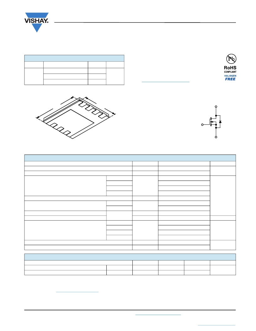
�PowerPAK� ?� SO-8�
�APPLICATIONS�
�?� Primary� Side� Switch�
�6.15� mm�
�1�
�S�
�S�
�5.15� mm�
�?� Isolated� DC/DC� Converters�
�?� Full� Bridge�
�D�
�2�
�3�
�S�
�4�
�G�
�8�
�D�
�7�
�D�
�6�
�D�
�D�
�G�
�5�
�Bottom� View�
�Ordering� Information:�
�SiR846ADP-T1-GE3� (Lead� (Pb)-free� and� Halogen-free)�
�ABSOLUTE� MAXIMUM� RATINGS� (T� A� =� 25� °C,� unless� otherwise� noted)�
�S�
�N-Channel� MOSFET�
�Parameter�
�Drain-Source� Voltage�
�Gate-Source� Voltage�
�T� C� =� 25� °C�
�Symbol�
�V� DS�
�V� GS�
�Limit�
�100�
�±� 20�
�60� a�
�Unit�
�V�
�Continuous� Drain� Current� (T� J� =� 150� °C)�
�T� C� =� 70� °C�
�T� A� =� 25� °C�
�I� D�
�58.6�
�18.6� b,� c�
�Pulsed� Drain� Current� (t� =� 100� μs)�
�Continuous� Source-Drain� Diode� Current�
�Single� Pulse� Avalanche� Current�
�Single� Pulse� Avalanche� Energy�
�T� A� =� 70� °C�
�T� C� =� 25� °C�
�T� A� =� 25� °C�
�L� =� ?� 0.1� mH�
�I� DM�
�I� S�
�I� AS�
�E� AS�
�14.7� b,� c�
�200�
�60� a�
�4.9� b,� c�
�40�
�80�
�A�
�mJ�
�T� C� =� 25� °C�
�83�
�Maximum� Power� Dissipation�
�T� C� =� 70� °C�
�T� A� =� 25� °C�
�P� D�
�53�
�5.4� b,� c�
�W�
�T� A� =� 70� °C�
�3.4� b,� c�
�Operating� Junction� and� Storage� Temperature� Range�
�Soldering� Recommendations� (Peak� Temperature)� d,� e�
�T� J� ,� T� stg�
�-� 55� to� 150�
�260�
�°C�
�THERMAL� RESISTANCE� RATINGS�
�Parameter�
�Symbol�
�Typical�
�Maximum�
�Unit�
�Maximum� Junction-to-Ambient� b,� f�
�Maximum� Junction-to-Case� (Drain)�
�t� ?� 10� s�
�Steady� State�
�R� thJA�
�R� thJC�
�18�
�1�
�23�
�1.5�
�°C/W�
�Notes:�
�a.� Package� limited.�
�b.� Surface� mounted� on� 1"� x� 1"� FR4� board.�
�c.� t� =� 10� s.�
�d.� See� solder� profile� (� www.vishay.com/doc?73257� ).� The� PowerPAK� SO-8� is� a� leadless� package.� The� end� of� the� lead� terminal� is� exposed� copper�
�(not� plated)� as� a� result� of� the� singulation� process� in� manufacturing.� A� solder� fillet� at� the� exposed� copper� tip� cannot� be� guaranteed� and� is� not�
�required� to� ensure� adequate� bottom� side� solder� interconnection.�
�e.� Rework� conditions:� manual� soldering� with� a� soldering� iron� is� not� recommended� for� leadless� components.�
�f.� Maximum� under� steady� state� conditions� is� 65� °C/W.�
�Document� Number:� 63823�
�S13-0829-Rev.� B,� 22-Apr-13�
�For� technical� support,� please� contact:� pmostechsupport@vishay.com�
�www.vishay.com�
�1�
�This� document� is� subject� to� change� without� notice.�
�THE� PRODUCTS� DESCRIBED� HEREIN� AND� THIS� DOCUMENT� ARE� SUBJECT� TO� SPECIFIC� DISCLAIMERS,� SET� FORTH� AT� www.vishay.com/doc?91000�
�发布紧急采购,3分钟左右您将得到回复。
相关PDF资料
SIR850DP-T1-GE3
MOSFET N-CH 25V 30A PPAK 8SOIC
SIR862DP-T1-GE3
MOSFET N-CH 25V 8-SOIC
SIR878ADP-T1-GE3
MOSFET N-CH 100V 40A POWERPAK
SIR878DP-T1-GE3
MOSFET N-CH 100V 8-SOIC
SIR888DP-T1-GE3
MOSFET N-CH 25V 40A PPAK 8SOIC
SIR890DP-T1-GE3
MOSFET N-CH 20V 50A PPAK 8SOIC
SIR892DP-T1-GE3
MOSFET N-CH 25V 50A PPAK 8SOIC
SIR928-6C-F
LED IR SIDE GAA1AS WATER CLR AXL
相关代理商/技术参数
SIR846DP
制造商:VISHAY 制造商全称:Vishay Siliconix 功能描述:N-Channel 100-V (D-S) MOSFET
SIR846DP-T1-GE3
功能描述:MOSFET 100V 60A 104W 7.8mohm @ 10V
RoHS:否 制造商:STMicroelectronics 晶体管极性:N-Channel 汲极/源极击穿电压:650 V 闸/源击穿电压:25 V 漏极连续电流:130 A 电阻汲极/源极 RDS(导通):0.014 Ohms 配置:Single 最大工作温度: 安装风格:Through Hole 封装 / 箱体:Max247 封装:Tube
SIR850DP
制造商:VISHAY 制造商全称:Vishay Siliconix 功能描述:N-Channel 25-V (D-S) MOSFET
SIR850DP-T1-GE3
功能描述:MOSFET 25V 30A 41.7W 7.0mohm @ 10V
RoHS:否 制造商:STMicroelectronics 晶体管极性:N-Channel 汲极/源极击穿电压:650 V 闸/源击穿电压:25 V 漏极连续电流:130 A 电阻汲极/源极 RDS(导通):0.014 Ohms 配置:Single 最大工作温度: 安装风格:Through Hole 封装 / 箱体:Max247 封装:Tube
SIR852160-WJ
制造商:CELDUC 制造商全称:celduc-relais 功能描述:New Solid State Relay compact size pitch 22,5mm with spring terminals
SIR862DP
制造商:VISHAY 制造商全称:Vishay Siliconix 功能描述:N-Channel 25-V (D-S) MOSFET
SIR862DP-T1-GE3
功能描述:MOSFET N-CH 25V 8-SOIC RoHS:是 类别:分离式半导体产品 >> FET - 单 系列:TrenchFET® 标准包装:1,000 系列:MESH OVERLAY™ FET 型:MOSFET N 通道,金属氧化物 FET 特点:逻辑电平门 漏极至源极电压(Vdss):200V 电流 - 连续漏极(Id) @ 25° C:18A 开态Rds(最大)@ Id, Vgs @ 25° C:180 毫欧 @ 9A,10V Id 时的 Vgs(th)(最大):4V @ 250µA 闸电荷(Qg) @ Vgs:72nC @ 10V 输入电容 (Ciss) @ Vds:1560pF @ 25V 功率 - 最大:40W 安装类型:通孔 封装/外壳:TO-220-3 整包 供应商设备封装:TO-220FP 包装:管件
SIR864DP
制造商:VISHAY 制造商全称:Vishay Siliconix 功能描述:N-Channel 30 V (D-S) MOSFET